|
Xiamen Powerway Advanced Material Co.,Ltd.
|
GaAs substrate
| Payment Terms: | T/T |
| Place of Origin: | Fujian, China (Mainland) |
|
|
|
| Add to My Favorites | |
| HiSupplier Escrow |
Product Detail
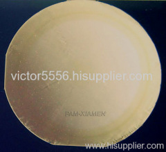
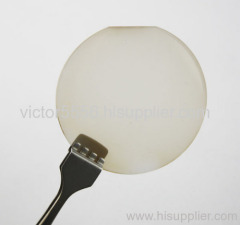
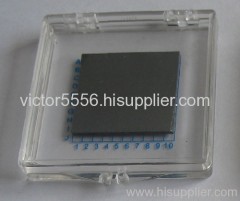
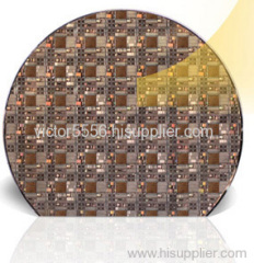
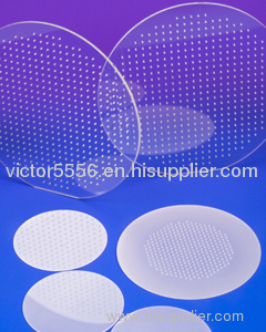
GaAs wafer, Gallium Arsenide wafer, GaAs substrate
PWAM Develops and manufactures compound semiconductor substrates-gallium arsenide crystal and wafer.We has used advanced crystal growth technology,vertical gradient freeze(VGF) and GaAs wafer processing technology,established a production line from crystal growth, cutting, grinding to polishing processing and built a 100-class clean room for wafer cleaning and packaging. Our GaAs wafer include 2~6 inch ingot/wafers for LED,LD and Microelectronics applications.
Didn't find what you're looking for?
Post Buying Lead or contact
HiSupplier Customer Service Center
for help!
Related Search
Find more related products in following catalogs on Hisupplier.com
Related Products

Company Info
Xiamen Powerway Advanced Material Co.,Ltd. [China (Mainland)]
Business Type:Manufacturer
City: Xiamen
Province/State: Fujian
Country/Region: China (Mainland)